Check out this comment for some tweaks to this guide to support the latest version of the tools!
Panelization is the process of taking two or more PCB designs and combining them using tabs or v-scores that you would then separate into individual boards once they come back from manufacturing. It’s a way to get more than one design made in a single order.
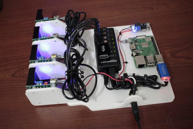
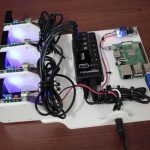
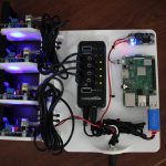
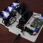
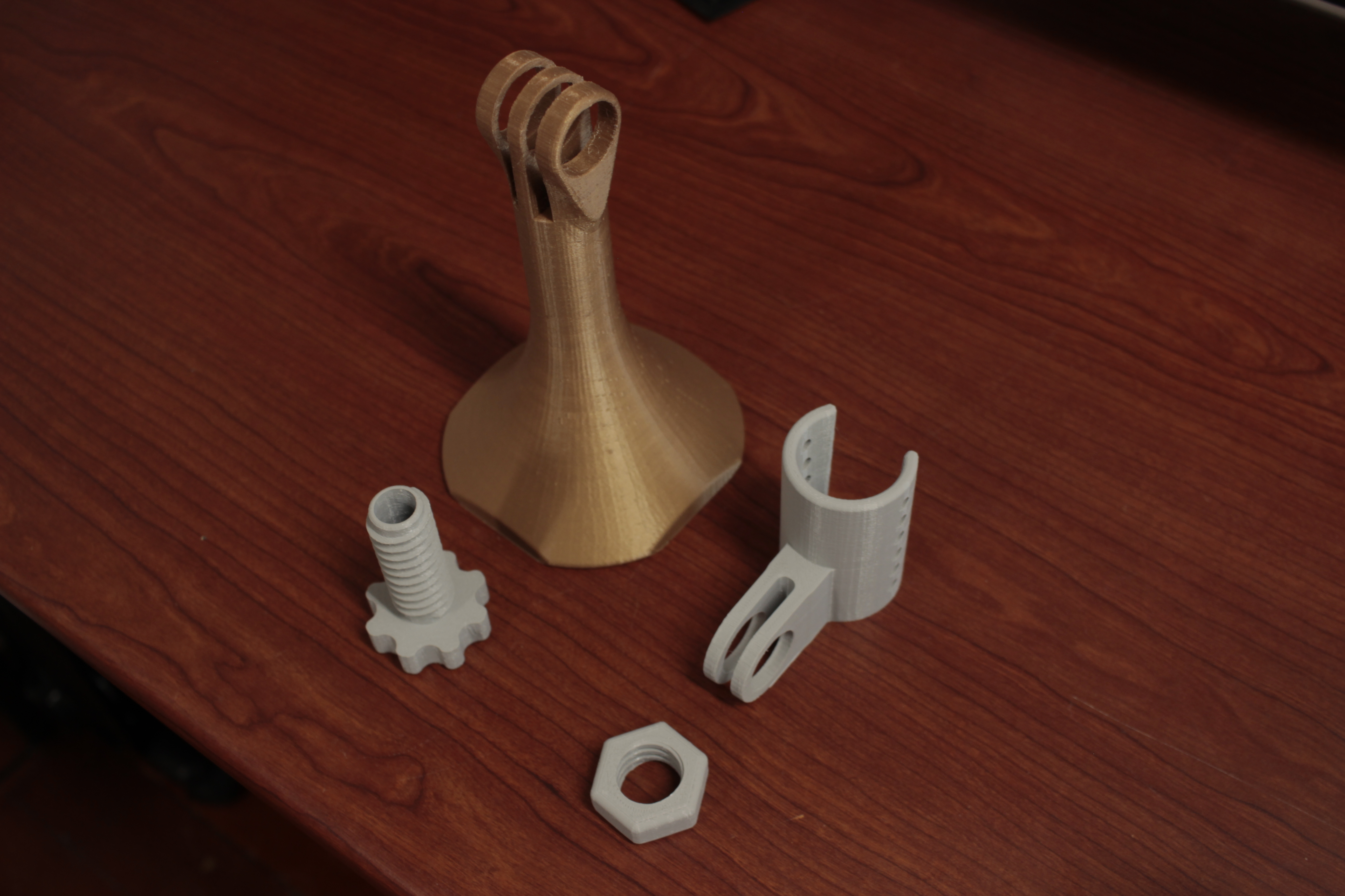
There are a few forum posts or other snippets on how to accomplish this out there already, but not a real guide. For my own sake, this is how you can do this panelization using all free tools. Here are some photos of a board I had fabricated by OSH Park using this panelization method:
I implement this technique whenever I’m creating closely-related PCBs.
The design highlighted in this blog post is a transmitter/receiver pair, meaning that there would never be a transmitter without a receiver, or vice-versa.
Design is made simple by doing the layouts individually, and manufacturing is made simple by getting them made as a single board, not having to coordinate multiple orders. Let’s get started with the guide.
1. Download The Tools
You probably already have KiCAD. Next, make sure to download GerberPanelizer by This is not Rocket Science (site link) from GitHub. This guide uses the 2018-08-10 snapshot release.
2. Export your designs from KiCAD
Your designs have to be completely ready for production before starting this process. Components placed, tracks laid, zones poured etc. It is very “one-way” in that it is impossible to update an already panelized design once it has been exported.
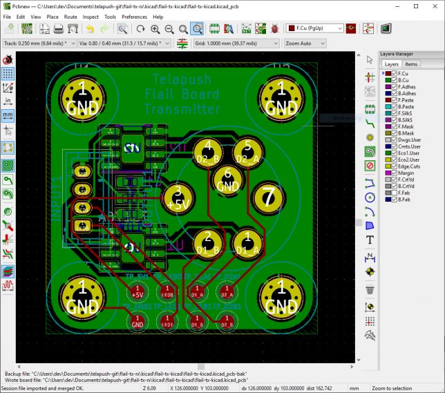
Here’s one of the designs that will be added to the panel.
You’ll want to add a grid origin that is really close to your design. In KiCAD, select place → grid origin to do this. I am putting it in the top left hand corner of the board.
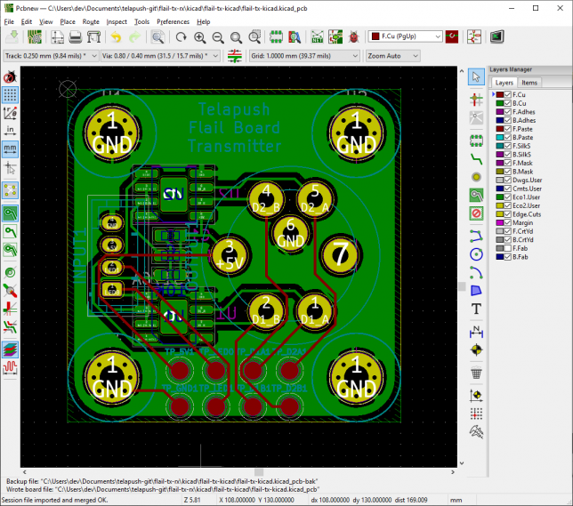
Grid origin placed
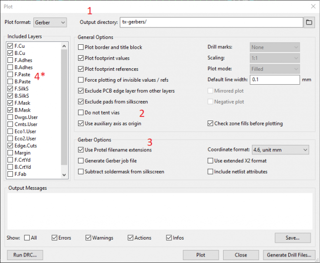
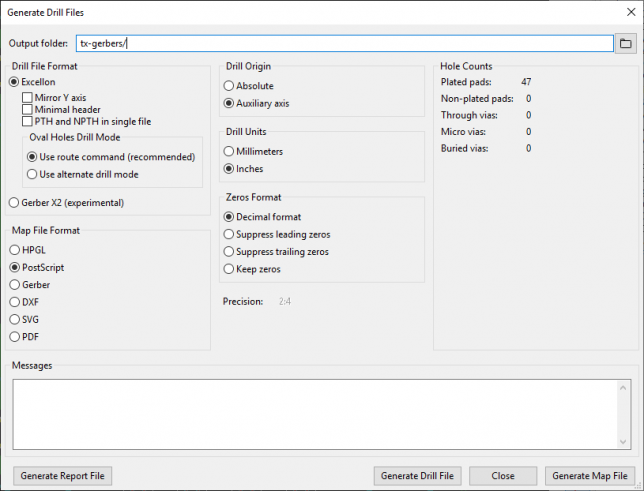
In pcbnew, select file → plot to adjust the gerber export settings.
- Make sure
Output directoryis set to an empty directory somewhere on your disk. In this example, it’s set totx-gerbers. - Check
Use auxiliary axis as origin - Check
Use Protel filename extensions - *Optional* Since I’m not using them in this design, I’ve unchecked
F.PasteandB.Paste.
And then click Plot.
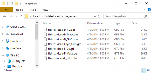
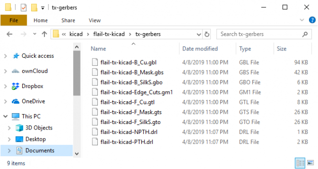
You should be greeted with a directory of files with dissimilar extensions:
Next, you need to export the .drlfiles.
Select file → fabrication outputs→ Drill (.drl) File...
These settings will automatically be set to match the previous export, but make sure the output folder and the drill origin match the previous settings. Mine looked like this:
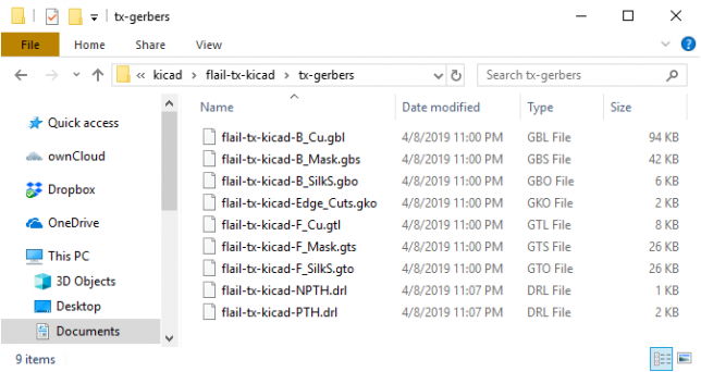
Here is my resulting output directory with all of the files:
3. Modify the exported files
This step is weird. You need to change the extension of all .gm1 files to .gko. For this example, flail-tx-kicad-Edge_Cuts.gm1 needs to be renamed to flail-tx-kicad-Edge_Cuts.gko as this is what GerberPanelizer expects. Here is my resulting directory:
.gko file4. Load the designs into Gerber Panelizer
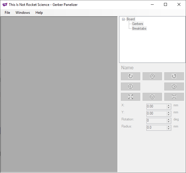
Open up GerberPanelizer, you will be greeted with this screen:
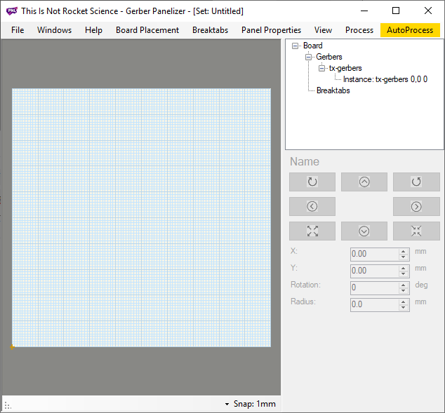
Select file → new to create a new project. Next, select board placement → add gerber folder and navigate to the output folder from KiCAD. In this example, it was tx-gerbers.
You should be seeing something like this:
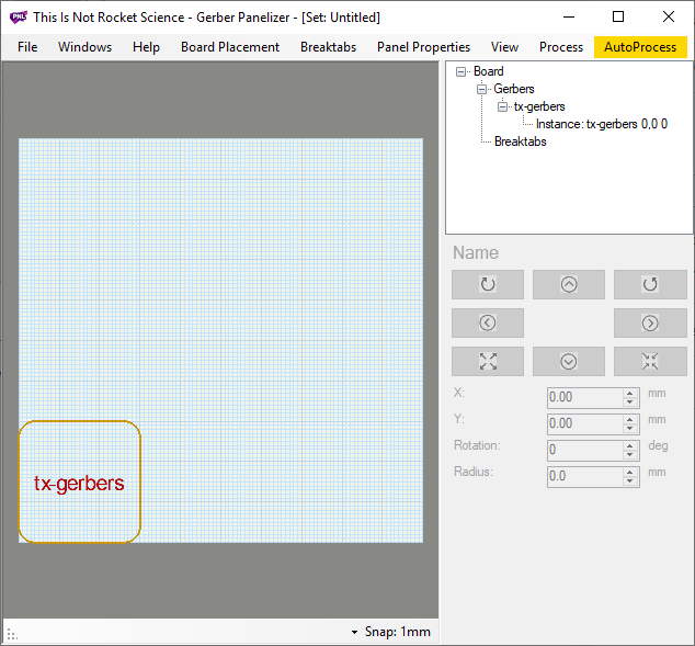
Where is the board?! Select board placement → autopack: native and your design will leap into view:
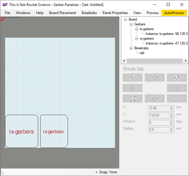
Now, re-do the guide up until this point for however many unique designs you want to add to this panel. If you want to duplicate your design multiple times in the same panel, you can add an instance by right clicking on the instance in the right hand view and then clicking add instance.
5. Arrange designs and add tabs
Since you’ve been hitting board placement → autopack: native after each board add, your designs should be properly arranged at this point. You can manually move the designs by clicking and dragging them, but I’ve found that using the autopack works really really well. Here’s what my design looks like at this point:

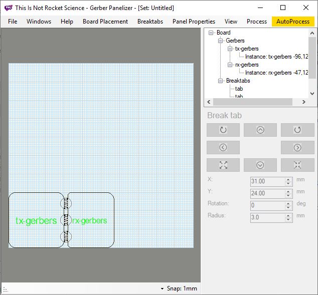
To join the designs together, you need to add breaktabs.
Select breaktabs → insert breaktab, and a small red circle will appear in the top left hand corner of the workspace:
Click and drag the tab between the two designs. Make sure black dots appear on either edge of the design:

Continue to add tabs in the same manner until the text turns a bright green color, this lets you know that the boards will be secured.
There is no way to automatically add the proper tabs, so make sure you use your best judgement.
Now we’re ready to export!
6. Export the panelized design
It’s a good idea to first save the design in GerberPanelizer so you can edit the layout later without having to start from scratch. Once you export the final merged gerber files, they cannot be edited or re-arranged. Select file →save as to save the project.
Now to export the gerbers.
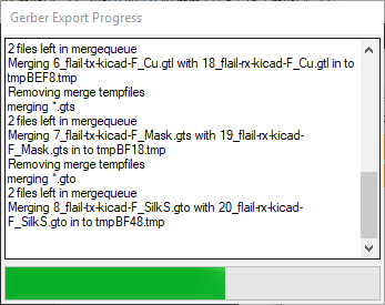
Again, in GerberPanelizer, select file → export merged gerbers and choose an empty output directory. The directory has to be empty because you typically send a zip archive of all gerbers to the manufacturer to get made, and this zip archive should just include this export. You should see this window pop up:
The contents of the merged output directory should look like this:
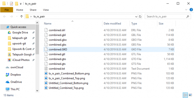
The merged output directory will include several image renderings of your merged designs, this is a great first check to make sure that everything went well.
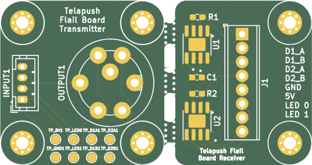
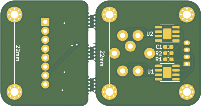
Looks good! However before you send any critical designs off for manufacturing it’s best practice to visually inspect the layers with a gerber viewer. Save the merged output directory as a .zip file.
7. Verify using GerbView
KiCAD ships with a program called GerbView to inspect gerber files. Open that gerbview and then open your zipped merged output directory with file → open zip archive file.
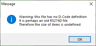
There will be an error message which you can ignore.
You should see something like this:
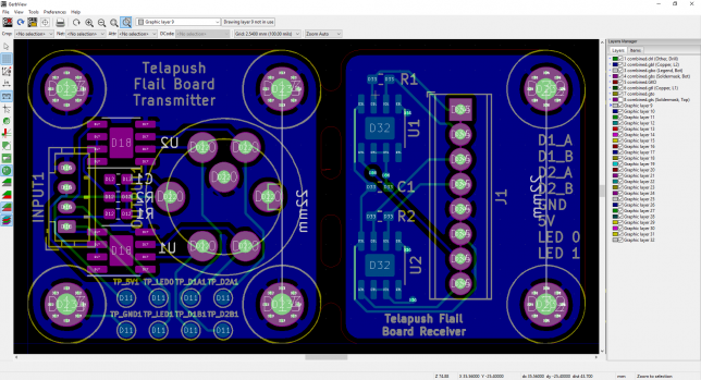
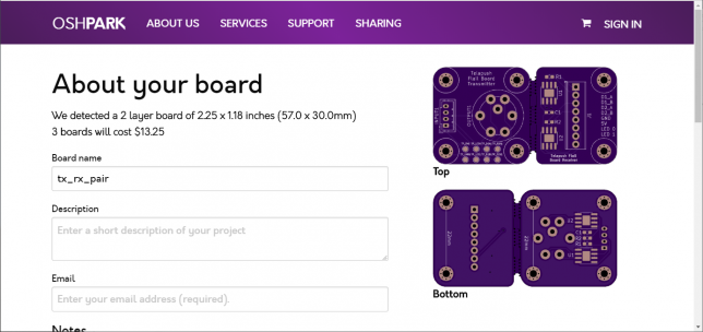
There’s the design as we expect it, you can uncheck the different layers on the right pane just like in pcbnew to inspect them one by one. I’ve uploaded this design to oshpark (a domestic PCB fab service) to see if their preview also looks correct and again, there are no problems.
You’re now ready to send your panelized designs out for manufacturing. Congrats!
8. Wrap up
Thanks for reading! Did this guide work for you? Let me know in the comments below this post.
Note: This is confirmed to work with KiCAD 4 and 5.


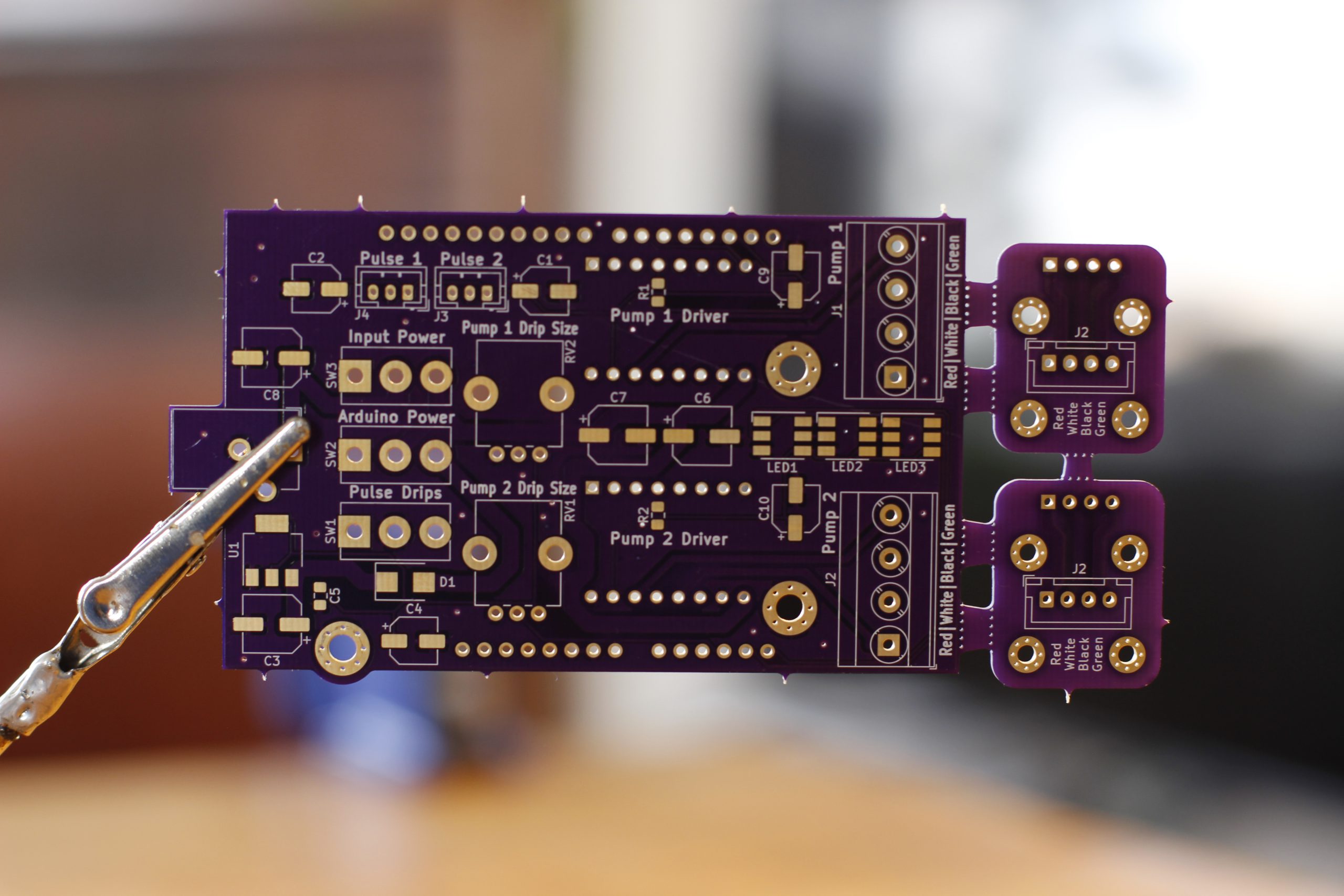
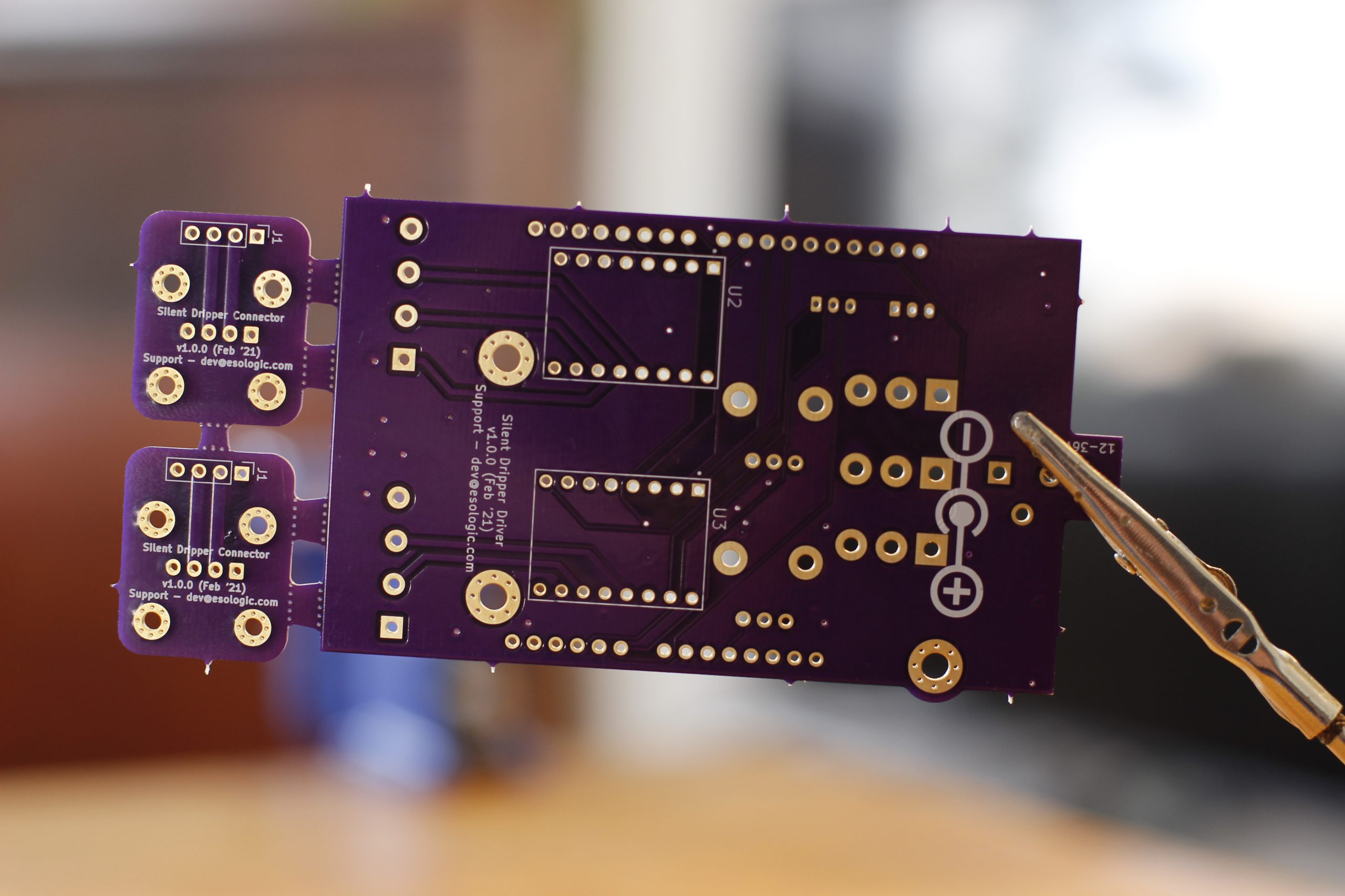
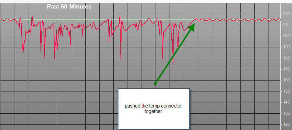 This seemed like a good place to start so I re-seated the connector and used